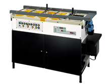
PCB 무전해 도금기
(응용 : 동도금, 금도금, 니켈도금 등 : 주문 제작 가능))
도금을 한번에 10장까지 가능 !!!
| THROUGH HOLE PLATING LINES |
|
ABC COPPER PLATE SYSTEM, SIMPLICITY ITSELF USING THE PL903/4 units
| PL903S |
Single PSU for Panel Plating - panel size 10" x
12" 50A |
| PL903D |
Double PSU for Pattern Plating - panel size 10" x 12" 100A
(2x50A) |
| PL904S |
Single PSU for Panel Plating - panel size 12" x 18".
100A |
| PL904D |
Double PSU for Pattern Plating - panel size 12" x 18" 100A
(2x50A) |
MAIN FEATURES
- Only 4 Process Functions, plus plating.
- Wide window of operation.
- Specially developed ABC Chemistry already being used by European PCB
Manufacturers.
- None of the nasty chemicals associated with other plating systems, (e.g.
no Formaldehyde).
- Line time less than one hour - half that of other systems. Stable
chemistry even when used irregularly.
- Minimum analysis - mostly done by replenishment (no specialist operator
required).
- Very compact equipment - ideal for use where space is limited.
- Solid state controls, dual current output - plating timer - re-settable
amp/hour counter.
In a major step forward Mega introduces a new concept for the production of
high quality Prototype and Production quantities of PTH boards. The process has
none of the complexities of older style methods of production which are both
time consuming and require expensive monitoring of processes on a daily basis.
The heart of the system is our patented chemistry which has only four processes
to prepare a panel to be electrolytically plated. Analysis of the chemistry is
minimal, maintenance being by replenishment on an amp hour basis. So simple is
the chemistry, we call it ABC. This new system features totally re-designed
electrolytic plating power supplies. They have controllers with membrane touch
pad and digital read out meters to set volts, current, plating time and amp
hours. It is also possible to set different current outputs to each side of the
board, (Twin PSU units only), essential for pattern plating especially where
larger areas of copper or ground planes are on one side and small tracks and
pads on the other.
 The two methods of producing a PTH board (PANEL PLATING
and PATTERN PLATING) are described below, both of which will produce high
quality boards. Pattern plating enables the board to be plated with a10-12
microns thick durable layer of lead/tin which can then be re-flowed to give a
bright shiny finish. Panel plating uses an immerse tin process which deposits
pure tin 1-2 microns thick which is ideal for prototypes and boards where a long
shelf life prior to soldering is not required.
The two methods of producing a PTH board (PANEL PLATING
and PATTERN PLATING) are described below, both of which will produce high
quality boards. Pattern plating enables the board to be plated with a10-12
microns thick durable layer of lead/tin which can then be re-flowed to give a
bright shiny finish. Panel plating uses an immerse tin process which deposits
pure tin 1-2 microns thick which is ideal for prototypes and boards where a long
shelf life prior to soldering is not required.
Processing Sequence
CLEANER / CONDITION (7 mins.) - Spray Rinse (1 min.) -
Pre-Dip (1/2 min.) - CATALYST (7 mins.) - Spray Rinse (1 min.) -SALT REMOVER (4
min.) - Spray Rinse (1 min.) - ELECTROLYTIC Cu (36 mins.)
| |
PL903S &
PL903D |
PL904S &
PL904D |
| Max. Panel Size: |
12" x 10" (305 x 254mm) |
18" x 12" (457 x 305mm) |
| Max.finished
PCB: |
11.5" x 9" (292 x 228mm) |
18" x 11" (457 x 280mm) |
| Tank capacity: |
Process 5L, Plating 25L |
Process 10L, Plating 50L |
| Rectifiers: |
PL903S 1 x 50A, PL903D 2 x 50A |
PL904S 1 x 100A, PL904D 2 x
50A |
| Agitation: |
Mechanical to all process
stages & air to plating |
| |
All
units |
| Dimensions: |
1500 x 620 x 910mm. |
| Electrics: |
Single phase 220/240V 50Hz or
110/120V 60Hz. |
| Heaters: |
500W Silica sheath. |
| Water in: |
Standard washing machine hose
fittings supplied. |
| Water out: |
36mm push fit polypropylene
drain. |
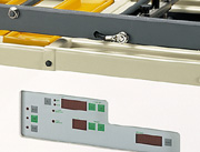
Power Supply Features - common to all copper and lead/tin plating.
- Independent Anode set current with digital meters.
- Set plating current time 0-99 minutes, digital.
- Pause facility - disconnects plating current at any period - pressing run
allows process to continue until plating time is completed.
- 0-9999 Digital Re-settable Amp hour meters.
- Sealed Membrane Front Panel Overlay with touch panel controls.
Rectifiers: PL903S 1 x 50A, PL903D 2 x 50A PL904S 1 x 100A, PL904D 2 x 50A
★ PCB 무전해도금기
|
|
PCB 무전해 도금장치 (A4용) 의 SET 구성표 (모델 : PLATING-A4)
|
|
1
|
전처리조 (350 X 250 X 300)
|
|
2
|
2단수 세조 (350 X 500 X 300)
|
|
3
|
도금조 (350 X 250 X 300)
|
|
4
|
2단수세조 (350 X 500 X 300)
|
|
5
|
후처리조 (350 X 250 X 300)
|
|
6
|
건조기
|
|
7
|
히터 (1.5W)
|
|
8
|
콘트롤러
|
|
9
|
BLOWER
|
|
10
|
기판랙 (300 X 200 X 400)
|
|
11
|
도금 기자재
|
|
|
간단하게 도금을 하거나 예산이 적을 경우 상기 품목에서 옵션들을
제외해도 됨
|
|
|
PCB 무전해 도금장치 (B4용) 의 SET 구성표 (모델 : PLATING-B4)
|
|
1
|
전처리조 (500 X 400 X 500)
|
|
2
|
3단수 세조 (500 X 1,200 X 500)
|
|
3
|
도금조 (500 X 400 X 500)
|
|
4
|
2단수세조 (500 X 800 X 500)
|
|
5
|
후처리조 (500 X 400 X 500)
|
|
6
|
건조기 (500 X 400 X 500)
|
|
7
|
히터 (2 W)
|
|
8
|
콘트롤러
|
|
9
|
BLOWER
|
|
10
|
기판랙 (300 X 200 X 400)
|
|
11
|
도금 기자재
|
|
|
간단하게 도금을 하거나 예산이 적을 경우 상기 품목에서 옵션들을
제외해도 됨
|
PCB용 무전해 도금장치
본 도금장치는 니켈, 동 등의 PCB 무전해 도금 전반에 걸쳐 활용할 수 있다. 본 장치는 전처리부터 건조까지 일체형으로 구성되어 있으며, 10장의 PCB를 동시에 무전해 도금이 가능하다.
1) 도금용 PCB 크기 : 210mm×297mm, 257mm×364mm [기타 size도 가능]
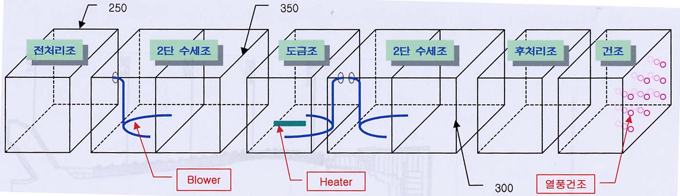
2) 구성 : 전처리조 + 수세조Ⅰ + 수세조Ⅱ + 도금조 + 수세조Ⅲ + 수세조Ⅳ + 후처리조/건조기
☞ 수세조Ⅰ, 도금조, 수세조Ⅲ에는 blower 장착
☞ 건조기는 열풍방식
3) 용량 : 각각 30 liter
4) 온도조절장치 : Ti heater, 상온-100C까지 조절
5) 재질 : PVC
6) Option
☞ PCB 거치대 : 10장까지 동시 처리 가능
☞ 음극진동장치 : 도금 표면조건 향상, 회전수 0~50회/분, 좌우회전거리 3~10cm
기타 사항(옵션)
1. 동도금, 무전해 금도금 등은 무전해 도금조와 동일함.
2. 무전해 도금을 평면으로 할 경우에는 blower 외에 음극진동 장치가 있어야 도금 표면의 균일성을 향상
3. 수세기는 다양한 종류가 있음
☞ 1차 수세에서 spray 형태로 기판을 세척하는 장치 추가
수세한 후에 랙을 꺼내면 자동으로 세척하는 장치가
있으며, 발판 등을 이용하여 수동으로 세척하는 타입이 있습니다.
☞ 전용 수세기 [전처리 및 후처리 가능, 약품을 이용하여 hole 등을 부드럽게 할 뿐만 아니라 기타 표면을 깨끗하게 처리 가능, 약 3~4m 정도]
당사는 반도체-PCB-LCD
장비는 물론 ITO GLASS, 폴리이미드필름 등 특수 에칭을 하여 양산으로 공급하고
있습니다.
반도체 - PCB - LCD - FPC
연구장비-생산장비, 실습-연구기자재, 전자재료 공급
스핀코터,마스크얼라이너, 4포인트프로브, 표면저항측정기, 와이어본더, 진공
펌프,
PCB샘플제작시스템,
디솔더링, 솔더링, Stencil Printer, BGA-SMD REWORK
SYSTEM, Wave soldering system, Reflow (리플로우 오븐)
선하야토 감광기판, 노광기, 현상기, 에칭기,
pcb에어졸, 키엔스센서, IC아답터 & 소켓,
레이저스펙트로미터, 전주도금기, 홀로그래픽, 스크라이버,
시편연마광택기(Polishing machine: Polisher),
핫 마운팅 프레스(Hot
Mounting Press machine), 시편 연마기(Belt Sander), 시편 절단기(Cutting Machine),
PCB코팅제-세정제, 전자부품-전자재료 공급.
TEL :
02-868-0661 (代)
pcb21@korea.com